Now loading...
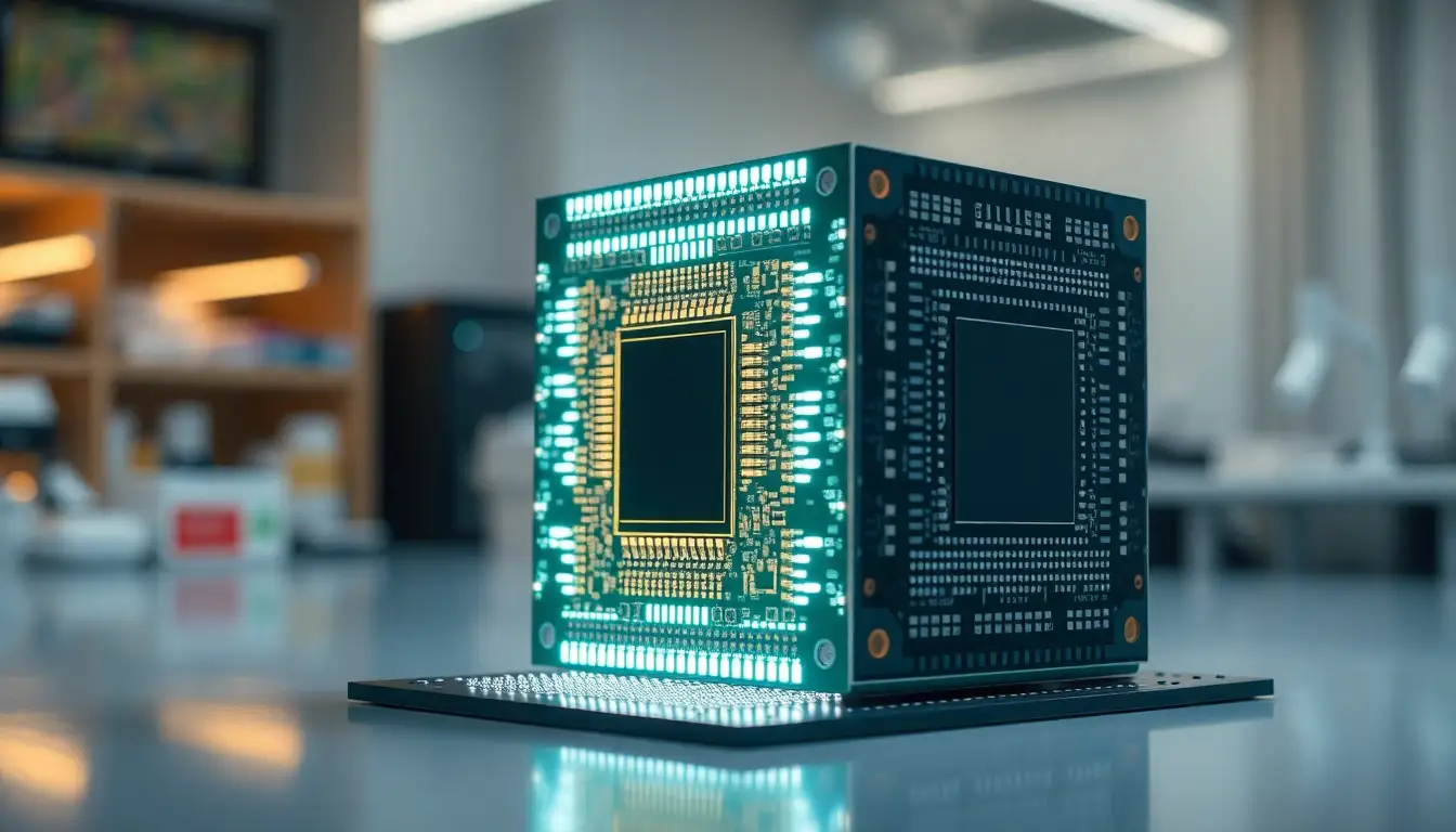
A team of engineers from top U.S. universities and a domestic semiconductor manufacturer has unveiled a pioneering three-dimensional computer chip that stacks processing and storage components vertically, promising significant boosts in speed for artificial intelligence applications.
The breakthrough, achieved by researchers at Stanford University, Carnegie Mellon University, the University of Pennsylvania and the Massachusetts Institute of Technology in collaboration with SkyWater Technology, marks the first fully integrated 3D chip fabricated entirely in a U.S. commercial facility. This monolithic design achieves the densest vertical interconnects yet recorded and delivers performance gains of about ten times over conventional flat chips, according to tests and models presented at the 71st Annual IEEE International Electron Devices Meeting.
Traditional two-dimensional chips arrange circuits on a single plane, creating bottlenecks as data shuttles between distant memory banks and processors. This setup, known as the memory wall, hampers efficiency in data-intensive AI tasks like those powering large language models. Meanwhile, efforts to pack more transistors onto chips are hitting physical barriers, dubbed the miniaturization wall.
The new chip counters these issues by layering ultra-thin circuit levels atop one another, with fine vertical links enabling swift data flow. By embedding memory close to computing elements, the structure reduces travel distances and congestion, much like multiple elevators in a skyscraper facilitating smoother resident movement.
Subhasish Mitra, a professor of electrical engineering and computer science at Stanford and lead investigator on the project, described the advance as a gateway to transformative chip manufacturing. He noted that such innovations are essential for the thousand-fold hardware leaps required by next-generation AI systems.
Tathagata Srimani, an assistant professor at Carnegie Mellon and senior author of the research, highlighted how vertical integration accelerates information transfer. His colleague Robert M. Radway from the University of Pennsylvania likened the dense stacking to a bustling urban grid, allowing more operations in a compact footprint.
Unlike prior 3D efforts that bond pre-made layers with limited connections, this approach fabricates each stratum sequentially at low temperatures to preserve underlying electronics. The result is a tighter, more reliable network produced at SkyWater’s Minnesota plant, underscoring U.S. potential in advanced semiconductor production.
Mark Nelson, vice president of technology development at SkyWater, emphasized the feat of translating academic ideas into scalable manufacturing. Initial prototypes already surpass two-dimensional counterparts by a factor of four, while projections for multi-layer expansions suggest up to twelve times faster processing on AI benchmarks, including variants of Meta’s LLaMA framework.
Looking ahead, the design could yield 100- to 1,000-fold enhancements in energy-delay product, a measure of efficiency blending speed and power use. Beyond raw performance, the work bolsters national capabilities in chip design and fabrication, supported by initiatives like the Microelectronics Commons California-Pacific-Northwest AI Hardware Hub.
H.-S. Philip Wong, a Stanford engineering professor and hub principal investigator, stressed that these developments not only elevate performance but also empower quicker innovation in AI hardware, training a new cohort of domestic experts.
The research received backing from agencies including the Defense Advanced Research Projects Agency, the National Science Foundation and the Department of Energy, highlighting its role in strengthening American technological leadership.
